Software for Embedded System Design and Development

| 0 comments |
Software for Embedded system design and development requires features that helps in creating as much as possible accurate system prototype from the designs specification(s). A typical embedded system requires from the hardware point of view- microcontroller(s), microprocessor(s), ADCs, DACs, DSPs, analog and passive components, digital components and possibly FPGA devices. Program for the microcontroller and microprocessor are required from the software point of view.

So software for embedded system design requires support for hardware components and interconnect and also support for program development.

A microcontroller or a microprocessor is at the heart of any embedded system so software should support wide variety of microcontroller/microprocessor available in the market, at least the popular ones. Besides the processors, additional parts required to co-work with the processors are required. These are sensors, transducers, passive and active analog components and digital components.

But besides these hardware components support, the software for embedded system design should have feature of programming the microcontroller/microprocessor. Creating optimized program for the embedded system is as much important as the design of the hardware architecture. There are many software for development program for microcontroller and microprocessor. Generally, compilers and assembler software are optimized for individual microprocessor and microcontrollers such as Keil for 8051 based microcontroller or MPLAB for PIC and so on. So to use the microcontroller one must buy them and learn them individually. This creates a curve in learning.

Now an example of a Software called Proteus is illustrated.

Proteus is a interactive Simulation Software for analog and digital design. Moreover,an added special feature of Proteus is that microcontrollers from wide variety of vendors can be simulated in real time. Those microcontrollers can be placed in the ISIS schematic editor, interconnected with peripheral device(s) and simulated to see the working of the microcontroller in real time. Of course, the microcontroller won’t do anything without a program writing to it. So proteus has facility to write, compile, debug and load program into the microcontroller. In short this is achieved by writing C program or assembly program and uploading the .hex,.exe or .asm file created by compiler or assembler program to the microcontroller on the schematics. Once you have done that, click the Run button and you have the microcontroller based embedded system running. It is also interactive simulation because you can have interactive push button or a keypad or others on the schematic connected to the microcontroller and when you press the switches or keys the outputs from microcontroller behaves according to the inputs.

Let’s illustrate with an example.

You start Proteus program and then you create a new project. Next you place the desired microcontroller onto the schematic ISIS editor. In this illustration example AT89C2051 microcontroller has been used. After placing the microcontroller, we can place desired devices to the microcontroller.

The following figure shows examples with single LED, multiple LEDs and a 7 Segment display connected to the port of the AT89C2051 microcontroller.
A single led is connected to the Port 1 of the microcontroller.


LEDs connected to the Port 1 of the microcontroller.


A 7 Segment display connected to the Port 1 of the microcontroller.


Now the software part will be explained.

Embedded System Design is not only about placing microcontroller in a schematic editor. The software must also be incorporate programming facilities so that the program written for the microcontroller can be verified and debugged.

With software such as Proteus, it allows a system designer to create program in C language and assembly language. With it’s own build in compiler and assembler it is pretty straight forward to write program and debug and verify it.

But the software is not limited to only developing it with its own compiler and assembler but also with other vendor software such as Keil for 8051 microcontrollers or PICC for PIC. IF you have the Keil or PICC program for example you can specify it at the time you start writing program, from within Proteus.

Following figure shows software development for the microcontroller using Keil compiler in Proteus.


Thus Proteus provides a essential feature of having both hardware and embedded software development support one might expect for Embedded System Design and Development. More tutorials on Interactive Microcontroller Simulation using Proteus using C language with Keil Compiler can be found in this blog- http://appliedelectronicsengineering.blogspot.com
Read More..

Half Wave and Full Wave Rectifier Simulation

| 0 comments |

Power Companies supplies an average rms AC voltage of 120V at a frequency of 60Hz to the civilian homes. This line voltage has to down converted to DC voltage required by electronics equipment. Transformers together with rectifiers is used in the electronics equipment for this purpose. Transformers only downconverts the magnitudes, that is, the signal at the output of the transformer or the secondary winding is still an AC signal with lower magnitude and the frequency is the same. This lowered AC signal is then converted to a subsequently converted to DC by full wave rectifier. Also after the full wave rectifier is a filter that smooths the noise DC signal from the full wave rectifier.

The voltage required at the rectifier side can be calculated using a formula that relates voltages, the inductance and turn ratio. This is given below-
[frac{V_2}{V_1}=frac{N_2}{N_1}=sqrt{frac{L_2}{L_1}}]
If we require a voltage of 50V at the secondary then V2=50 and V1=120V. If we take primary inductor value as L1=10mH then the formula above gives L2=1.73mH.

Using these values we can stimulate how the AC signal conversion happens with the transfomer design. Shown below is a schematic for simulation for the verification of operation of transformer action in Orcad capture.
In the above schematic, the AC source signal enters the transformer with the calculated inductor values above. The resistors of 0.2ohm are there to model the small resistance values of the inductor. The K linear part is required in Orcad capture, and with this part we can specify the strength of the coupling. Here the coupling strength is 0.9, so 90% is coupled from the primary to secondary and 10% is lost in the air core(say). Orcad capture also requires a dc path to ground. This is provided by a high resistance wire of 1Gohm path.

Now a simulation of this circuit gives us a waveform graph as shown above.


The graph shows the voltage at the primary side in red and the voltage at the secondary side in green. We observe that the circuit did reduce the voltage but not down to 50V. The observed voltage is 41 to 42V. This is because of the coupling strength provided as 0.9. If we put the strength as 1 then the voltage does convert to 50V exactly. Also the down converted voltage is still an AC signal.

Lets change the coupling strength to 0.999 so that we get a 50V at the secondary circuit.


Now re stimulate the circuit gives us the following waveform graph.


The signal at the secondary has become larger to 50V.

Next we will add a diode to the secondary circuit to see its consequence.


Read More..

2 to 1 multiplexer verilog code using conditional operator Verilog tutorial

| 0 comments |
This verilog tutorial shows how a 2 to 1 multiplexer can be designed in verilog using conditional operator"?". This way of implementing a circuit in verilog is called behavioral modelling. A multiplexer can also be modelled using strucural modelling which was illustrated in earlier blog post 2 to 1 multiplexer Verilog Code


Verilog code for 2 to 1 multiplexer using Conditional Operator

module mux2x1(a, b, sel, z);
    input a, b, sel;
    output z;
   
    assign z = sel? a:b;
   
endmodule

The input to the multiplexer is a and b. sel is the selector signal and z is the output. assign statement is used to assign input a or b to output z according to value of sel signal.

If sel is logic 0 then z = b and if sel is logic 1 then z = a.


Compilation and Simulation Result:

The code was compiled and simulated using verilog Software and the simulation trace is shown below:


Related Simulation:

See also VHDL code for the 2 to 1 multiplexer:

VHDL code for 2 to 1 multiplexer using when, select, if, case statements and structural model

Read also 2 to 1 multiplexer simulation in Proteus Professional:

4x1 and 2x1 multiplexer circuit simulation
Read More..

Kontak

| 0 comments |
______________________________________________________
 teukuiwan
_______________________________________________________

Teuku_Mirwan
________________________________________________________
085270858522
____________________________
infoteukuiwan@gmail.com
_______________________________________________________
PIN : Teuku Mirwan Sahputra
  
Read More..

How on build your own Transformers Robots Robots Androids and Animations

| 0 comments |
This summary is not available. Please click here to view the post.
Read More..

A Frightening Experience

| 0 comments |

This happened while I was gone to Ohio for summer vacation last year. I decided to be brave and go on another coaster for the second time in my life. I find that funny. Ive decided to write a narrative from the top of my head about the experience. I know there are times when we all get scared to do the unimagined, but we have to face that fear and overcome it. Cedar Point is an awesome place to go with family and friends.

An experience riding a rollercoaster with big, frightening drops made me think twice about riding another coaster. When I first stood in line, it was very long, but I ended up on the coaster in less than an hour. After I had stood in line as long as I did, I was excited about riding the rollercoaster. However, When I finally got my change to take my seat, I wanted to get off. Instead, I decided that I was going to stay on it. Finally, the ride left the station, and I was excited. I sat in the seat, and the first drop came; I scream. This ride scared me as it went up and down the wood tracks, In seconds, the ride was over, and I hopped out of my seat. Although it was frightened from the ride, it turned out to be a fun experience for me.

Read More..

How to convert between data types in VHDL

| 0 comments |
There are basically 4 data types you will encounter in vhdl programming. They are std_logic_vector, unsigned, signed and integers. Normally you would define the interface or ports as std_logic_vector. But while you create hardware that does certain function you need to convert the std_logic_vector to unsigned, signed or integer and back from these to std_logic_vector. The std_logic_vector are simply binary bits which have no information about the mathematical form such as signed or unsigned integer.

Thus we often need to convert the incoming binary bits to unsigned, signed integers. For example if the input bits are numbers on which we want to perform arithmetic operation then we want to convert these input binary bits to unsigned or signed integer and then we can use the mathematical operators.
Mathematical operators like +, -, * and / can be used in the concurrent or sequential statements.

Consider for example that your are designing an arithmetic hardware that takes as inputs two signals a and b of data type std_logic_vector.

If x is a std_logic_vector data type then to convert it to unsigned or signed use-
unsigned(x)
signed(x)

If x is unsigned or signed data type then to convert it to std_logic_vector use-
std_logic_vector(x)

If x is an unsigned or signed then to convert unsigned or signed to integer then use-
to_integer(x)

If x is an integer then you can convert it to unsigned or signed use-
to_unsigned(x,size)
to_signed(x,size)

Read More..

Positive and Negative Edge Triggered D flip flop with VHDL example

| 0 comments |
A synchoronous system is one which contains elements which can be triggered to change internal state by applying clock pulse to the internal register of a synchronous system. That is the internal registers or flip flops are synchronized to a common clock.

A synchronous system is made of registers which are in turn made of flip flop. There are various types of flip flop such as SR flip flop, JK flip flops, D flip flop. D flip flop are commonly used in the design of synchronous system. One reason is that D flip flop operates with single input while SR and JK flip flop operates with two inputs.

A D flip flop can be modelled in VHDL in many ways. Here 3 ways of modelling a D flip flop is shown. The VHDL models are simulated using aldec VHDL software.

A D flip flop symbol diagram in proteus professional circuit diagram editor is shown below.

d flip flop


As mentioned earlier latch is level triggered storage device while a flip flop is edge triggered device. The input to the latch is a pulse whose level of logic(usually high) is detected and the the stored bit appears at the output. The flip flop such as D flip flop are driven by the clock input whose edge transition from low to high called positive edge triggered or high to low transition called negative triggered is detected.

Now we will illustrate how to model a D flip flop in VHDL. 3 different ways of modelling a D flip flop will be shown.

First model of D flip flop:

First we will consider positive edge triggered D flip flop.

The first model model1 VHDL code is below. Here sequential process statement without sensitivity list and using wait until statement is used. The wait until statement causes the edge detection.

library ieee;
use ieee.std_logic_1164.all;

entity DFFmodel1 is
    port(
    D, clk : in std_logic;
    Q : out std_logic
    );
end DFFmodel1;

architecture model1 of DFFmodel1 is
begin
    pro : process is
    begin
    wait until (clk = 1);
    Q <= D;
    end process pro;
end model1;

In the above D flip flop model1,the process is not evaluated until clock signal is logic high. Once clock signal goes high(rising edge) the next assignment statement Q<=D is evaluated. This is repeated in the next rising edge of the clock.

The simulation waveform is shown below,

positive edge triggered D flip flop simulated waveform

In the above waveform diagram, the input to the flip flop D occurs in the 5th clock cycle but does not appear at the output at this 5th clock cycle. The output at Q appears in the 6th clock cycle on the rising edge of the clock signal.

Second model of D flip flop

This second method uses if then statement within a process with sensitivity list. The if (condition) is the edge detection in this case.

library ieee;
use ieee.std_logic_1164.all;

entity DFFmodel2 is
    port(
    D, clk : in std_logic;
    Q : out std_logic
    );
end DFFmodel2;

architecture model2 of DFFmodel2 is
begin
    pro : process(D,clk)
    begin
    if (clk = 1) then
    Q <= D;
    end if;
    end process pro;
end model2;

In this case notice that there is no wait statement like in the first model.

The simulated waveform in vhdl software aldec is shown below,

positive edge triggered D flip flop simulated waveform

This waveform is same as the first one.

Third Model of D flip flop

The 3rd model vhdl code is same as the second but with sensitivity list removed and wait on statement added in the end of the process.

library ieee;
use ieee.std_logic_1164.all;

entity DFFmodel3 is
    port(
    D, clk : in std_logic;
    Q : out std_logic
    );
end DFFmodel3;

architecture model3 of DFFmodel3 is
begin
    pro : process
    begin
    if (clk = 1) then
    Q <= D;
    end if;
    wait on clk;
    end process pro;
end model3;

So this model is like a compromise of the 1st and 2nd model. Here the wait on statement acts like the sensitivity list of a process whose function is to re-evaluate if there is any change of the signal within the sensitivity list.

The waveform will be same as that shown in the above two models(1 and 2).

There is some differences of the 3 models that were illustrated. Before we explain that one must remember that a process can have either sensitivity list or one or more wait statement but not both. VHDL software will error if this happens. As a substitute, one can replace the sensitivity list with wait on statement was was done in the 3rd model.

All of the above model were positive edge triggered D flip flops.

Now at last, we want to show negative edge triggered D flip flop VHDL modelling.

The following code shows this,

library ieee;
use ieee.std_logic_1164.all;

entity negDFFmodel1 is
    port(
    D, clk : in std_logic;
    Q : out std_logic
    );
end negDFFmodel1;

architecture model1 of negDFFmodel1 is
begin
    pro : process is
    begin
    wait until (clk = 0);
    Q <= D;
    end process pro;
end model1;

The following is the simulated waveform. Compare this with the positive edge triggered D flip flop simulated waveform above.

negative edge triggered D flip flop simulated waveform

The data D appears at the output Q at the falling edge of the 6th clock pulse.

Similarly we can write the vhdl code for the negative triggered flip flop by replacing the 1 by 0 in the 2nd and 3rd model.
Read More..

Piriform Defraggler v1 13 155 Full Portable Multilenguaje

| 0 comments |
Que un programa esté creado por los autores de CCleaner o Recuva, es toda una garantía. Este es el caso de Defraggler, un interesante desfragmentador de archivos y discos duros.

La ventaja principal de la que hace gala Defraggler es que puedes ir directo al archivo que más te interese (o carpeta), desfragmentándolo sin tocar el resto.

Por otro lado, si lo que quieres es desfragmentar todo el disco duro entero, también puedes hacerlo con Defraggler. Analízalo y elige la acción "Defrag Drive".
[Ver post]

Resulta especialmente interesante que, si seleccionas un archivo, puedes ver claramente lo fragmentado que está. También puedes ordenar por número de fragmentos, así se localiza rápida y fácilmente los archivos más fragmentados.

Sistema operativo:
Win2000/XP/2003/Vista/7

Defraggler v1.13 Nueva Actualización:
-Áñadido desfragmentador rápido a la versión de línea de comandos
-Correcciones
-Mejor velocidad cuando se mueven archivos grandes al final de la unidad


Descarga:

Piriform Defraggler v1.13.155 Full:
RapidShare/desde Defraggler


Piriform Defraggler v1.13.155 Portable:
RapidShare


(Clic en la imagen para descargar)

Read More..

How to measure and place components at the edge of PCB board

| 0 comments |

How far the components should be placed from the edge of the PCB board is things that are often asked by PCB beginners. This tutorial shows how in Altium designer how one can measure the distance between the component and the distance between the component and the edge of the PCB board so that one knows where to place the component.

There are standards such as IPC standards that dictates the distance between the components, between the components and the edge for different types of components such as axial or radial, through hole or surface mount and for discrete, IC etc.

Below shows a typical example of how to measure and place distance dimension in a PCB layout in altium designer. Suppose we have an initial PCB board like the one shown below.


The picture above shows series of through hole resistors placed along the edge of the PCB board. We dont know how far the left most resistor is placed from the two edges of the board. Here we can use the standard dimension tool in altium designer. This tool can be activated and used from the toolbar. It is available in the under utility as Place Standard Dimension.


 The distance from the right side edge is 3.3mm. The minimum recommended distance from side of the PCB board is 1.9mm. The distance is well within the recommended distance from the edge. So we can go move the resistor more closer to that side of the edge.

Similarly, the distance of the center of the pad of the resistor to the bottom edge of the PCB board is 4.216 which is also within the recommended distance of 2.29,


Now lets check the side to side distance between the pads of the resistors R11 and R9. This distance should have a minimum separation of 2.54mm.


 The measure distance is 4.115mm which is also within the recommended spacing between the discrete axial THD component. So for example if there is scarcity of space in the PCB board or if the design should be made small we could place them closer without worrying about the possibility of damaging the devices when soldering them.

Another component placement is the placement of discrete radial THD such as electrolytic capacitor. The board has an electrolytic capacitor placed at the edge of the PCB board as shown below.


The measured distance of the electrolytic capacitor from the edge is 3.353mm which is also within the recommended distance from edge which is greater than the half of the diameter of the electrolytic capacitor or the radial THD device or r> 1.52mm.


This altium designer tutorial showed you how to place components at the edge of the PCB by marking the distance in PCB layout using the standard dimension tool in altium designer.
Read More..

3D visualization of a function with Matlab

| 0 comments |


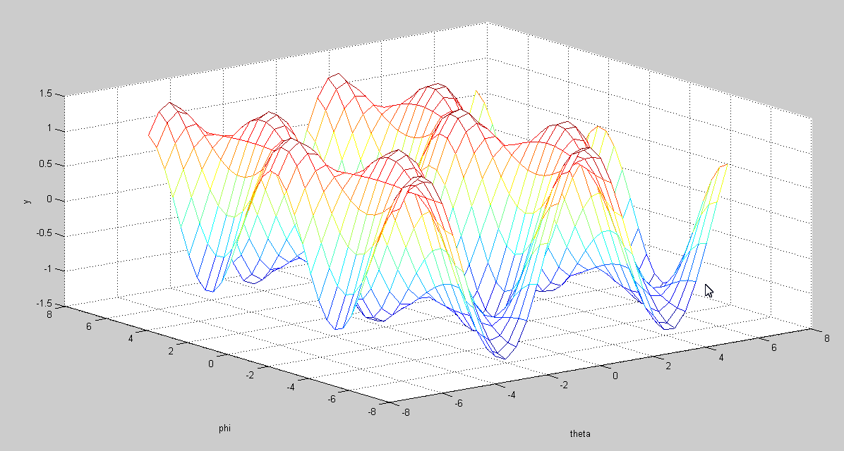
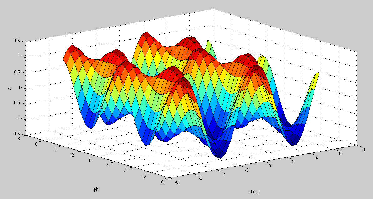
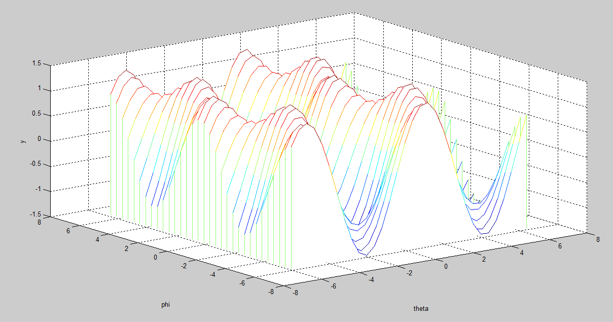
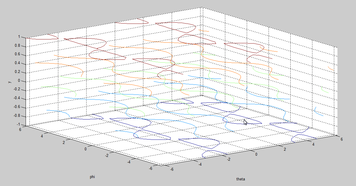
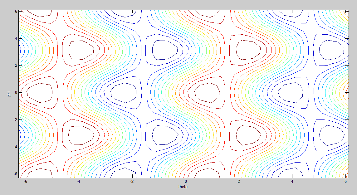
Matlab provides a number of functions that can be used to plot a function of 2 variables. Consider the following function.

y = sin(theta)+ cos(phi).*cos(theta)

here y is dependent on two variables theta and phi.
 
Now using 3D visualization tools in matlab the function will be plotted. This can be plotted in 3d graphics with matlab.. First define the grid on the xy plane as follows.

[theta, phi] = meshgrid(-2*pi:0.4:2*pi, -2*pi:0.4:2*pi);

Then define the function y,


y = sin(theta)+ cos(phi).*cos(theta);

Then use the various 3d plot functions as follows,

figure(1)
mesh(theta, phi, y)
xlabel(theta); ylabel(phi); zlabel(y)


 figure(2)
surf(theta, phi, y)
xlabel(theta); ylabel(phi); zlabel(y)


figure(3)
surfc(theta, phi, y)
xlabel(theta); ylabel(phi); zlabel(y)


 figure(4)
waterfall(theta, phi, y)
xlabel(theta); ylabel(phi); zlabel(y)


figure(5)
contour3(theta, phi, y)
xlabel(theta); ylabel(phi); zlabel(y)


figure(6)
contour(theta, phi, y, 15)
xlabel(theta); ylabel(phi); zlabel(y)


Read More..

The Intel 8255A IC programming modes

| 0 comments |
The intel 8255A IC is a PPI(Programmable Peripheral Interface) IC that is used for parallel communication interfacing between a CPU such as intel 8085 and I/O devices such as printer or keyboard. The Intel 8255 has two functional mode which are Bit Set Reset(BSR) mode and the I/O mode. The I/O mode has futher 3 modes which are generally called mode 0, mode 1 and mode 2. The mode 0 is also known as simple I/O mode, mode 1 is known as handshaking mode and mode 2 is called bidirectional mode.

In Bit Set Reset(BSR) mode, the port C pins are can be individually set or reset. The mode 0 or simple I/O mode is the ports configuration in which the port A and port B are used for either simple input or output ports and the port C port is used for handshaking. In mode 3 or bidirectional mode, the port A is used for bidirectional port with C port bits as handshaking while port B is used in simple I/O port(mode 0) or handshaking(mode 1).

To configure the 8255A ports we write control word and send it the control register from the CPU like intel 8085 via the data bus. The control word bits are such that when the MSB of the 8 bit word is 0 then it indicates BSR mode and when it is 1 then it indicates I/O mode. Thus the first bit of the control word is for choosing which of the primary functions, that is, BSR or I/O mode is to use.

If in case BSR is chosen so that the first bit is 0, then the 7th, 6th and 5th bits are dont care which means that it doesnt matter whether they are 1 or 0 bit. Then the next 4th, 3rd and 2nd bit combination selects the 8 pins of the port C. This means that upon the selection of the combination of the 4th, 3rd and 2nd bits we can choose which one of the port C pin to set or reset. The 1st bit or the LSB is for set or reset. That is 1 indicates set and 0 indicates reset.

If in case I/O mode is selected so that first bit is 1, then remaining 7 bits of the control words is to configure-

- port A either as mode 0, mode 1 or mode 2, and either as input or output port
- port B either as mode 0 or mode 1 and either as input or output port
- port C either as input or output

The simple I/O mode or mode 0 configuration is the simplest control word configuration. The handshaking mode/ mode 1 is the more difficult which is explained next.

In the handshaking mode, port A and port B can be configured as either input or output port. The port C pins are used for handshaking control signals which are STB active low, IBF active high and INTR if the port is configured as input port and OBF active low, ACK active low and INTR active low.


There are 8 pins of port C which are configured depending whether the port A and port B are input or output.

If for example A and B ports are configured as input port then,

PC7 - either input or output
PC6 - either input or output
PC5a - IBFa
PC4a - STBa
PC3a - INTRa
PC2b - STBb
PC1b - IBFb
PC0b - INTRb

where indicates active low signal and a, b indicates port A and port B

If A and B ports are configured as output port then,

PC7a - OBFa
PC6a - ACKa
PC5 - either input or output
PC4 - either input or output
PC3a - INTRa
PC2b -ACKb
PC1b - OBFb
PC0b - INTRb

Thus when the port A is an input port in the mode 1 configuration then PC5, PC4, PC3 are reserved. Similarly when port A is an output port in mode1 then PC7, PC6 and PC3 are reserved. In case of port B this is not the situtation, that is whether it is a input or output PC2, PC1 and PC0 are reserved for port B.

The final mode is the mode2 or  the strobe bidirectional bus I/O mode. In this mode only the port A can be used for bidirectional 8 bit I/O bus using the port Cs PC7 to PC3 for handshaking. Port B can be programmed only in mode0 or mode1. In case port B is configured as mode0 then PC2 to PC0 is used for input or output and in case it it configured as mode1 then PC2 to PC0 are used for handshaking.


Read More..

Memaknai Bulan Ramadhan

| 0 comments |

Ramadhan adalah bulan yang istimewa bagi setiap mukmin. Berikut ini beberapa keistimewaannya bulan ramadhan:

1.  Ramadhan adalah rabi’ul hayat (musim semi kehidupan) bagi setiap muslim dan bagi umat ini.
Sebagaimana musim semi dimana daun-daun kembali tumbuh dan bunga-bunga bermekaran, setelah sebelumnya kering kerontang, udara menjadi segar setelah sebelumnya kering menusuk tulang, maka demikianlah ramadhan. Di bulan ramadhan, pikiran kita disegarkan kembali dengan banyaknya taklim di masjid-masjid, di kantor-kantor, di radio, di televisi, di surat-surat kabar.
Pikiran kita diajak kembali untuk memahami ajaran agama kita. Di bulan ramadhan, rohani kita disegarkan kembali dengan bacaan Al-Qur’an, sholat tarawih, dan puasa itu sendiri. Di bulan ramadhan, jasad kita pun disegarkan kembali dengan puasa, yang menurut para ahli kesehatan dan medis, bisa menetralisir racun-racun dalam tubuh, dan secara umum sangat baik untuk kesehatan tubuh. Keluarga-keluarga muslim juga dieratkan dengan berbuka, makan sahur bersama, dan sebagainya. Umat Islam secara keseluruhan juga dieratkan dengan saling tolong menolong, memberi infaq, zakat dan shadaqah, dan saling bersilaturahim.

2.  Ramadhan adalah bulan penghapusan dosa.
Dahulu, para salafunash shalih, generasi terdahulu umat ini, jika ramadhan akan datang, mereka mengucapkan: marhaban bil muthahhir “selamat datang bulan penghapus dosa”. Mengapa? Karena selama sebelas bulan sebelum ramadhan telah banyak dosa dan kesalahan yang telah diperbuat, dan ramadhan adalah kesempatan emas untuk memohon ampunan dari Allah.
Ramadhan adalah sarana penghapusan dosa yang bersifat tahunan. Sebagaimana sabda Rasulullah saw: ”Dari ramadhan ke ramadhan, dari jum’at ke jum’at, dan dari sholat lima waktu ke sholat lima waktu yang lain, adalah sarana penghapusan dosa.” Dan tidakkah kita dengar sabda Rasulullah saw: “Barangsiapa yang berpuasa ramadhan atas dasar iman dan berharap-harap ridha Allah, maka akan diampuni dosa-dosanya yang telah lalu.” “Barangsiapa yang menghidupkan malam-malam ramadhan dengan sholat (tarawih) atas dasar iman dan berharap-harap ridha Allah, maka akan diampuni dosa-dosanya yang telah lalu.” “Barangsiapa yang menghidupkan malam Lailatul Qadar  dengan sholat (tarawih) atas dasar iman dan berharap-harap ridha Allah, maka akan diampuni dosa-dosanya yang telah lalu.”

3.  Ramadhan adalah bulan kesabaran.
Dengan ramadhan, kita dilatih untuk menjadi manusia yang sabar, artinya: yang bisa mengendalikan diri. Dan dengan kemampuan mengendalikan diri inilah, kita bisa berbeda dengan binatang. Jika ada seekor binatang mendapati makanan kesukaannya di tengah jalan, apa yang akan ia lakukan? Apakah ia akan menimbang-nimbang dulu: bolehkah makanan ini aku santap? Tentu ia akan langsung saja menyantapnya tanpa pernah berpikir boleh dan tidaknya, apalagi pantas dan tidaknya.
Di bulan ramadhan, makanan dan minuman yang jelas-jelas halal saja tidak kita makan, meski kita sedang lapar dan sedang kehausan. Semata-mata karena perintah Allah. Jika makanan yang halal saja kita hindari, apalagi makanan yang haram? Dan dalam kehidupan kita sekarang ini, kita lihat betapa banyak orang – yang bahkan muslim – memakan yang haram. Yang diperoleh dengan menipu, mencuri, korupsi, manipulasi, penggelapan, bahkan merampok dan menodong.
Di bulan ramadhan, istri yang jelas-jelas halal saja dijauhi. Maka apalagi wanita yang tidak halal? Sementara saat ini kita melihat betapa banyak orang – yang bahkan muslim – yang melakukan zina dengan wanita yang tidak halal baginya. Inilah ramadhan, yang akan melatih diri kita untuk sabar: bisa mengendalikan diri.

4.  Ramadhan adalah bulan untuk berbekal.
Wa tazawwaduu fainna khairaz zaadit taqwaa (Dan berbekallah kalian. Maka sesungguhnya sebaik-baik bekal adalah taqwa). Dan bulan ramadhan ini tidak lain adalah la’allakum tattaquun, untuk meraih derajat taqwa. Karena itu ramadhan semestinya dijadikan sebagai waktu khusus penyiapan bekal untuk sebelas bulan berikutnya sesudah ramadhan. Ini tidak ada bedanya seperti men-charge baterai ponsel kita. Karena itu, ramadhan yang benar adalah jika kebaikan dan ketaatan kita bisa terus berlanjut sesudah ramadhan. Dan itu adalah indikasi bahwa ramadhan kita diterima.
Jangan sampai kita menjadi orang-orang ramadhani, yaitu penyembah bulan ramadhan, yang hanya baik ketika ramadhan saja. Begitu ramadhan lewat, kita tidak lagi menjadi baik. Sebaliknya, jadilah orang-orang yang rabbani, yaitu penyembah Rabb (tuhan kita), yaitu Allah swt. Sebagaimana Allah selalu ada, maka kita juga selalu baik meski ramadhan telah lewat.
Kita semua adalah musafir, dengan tujuan negeri akhirat. Karena kita musafir maka kita perlu perbekalan. Wa tazawwaduu fainna khairaz zaadit taqwaa. Dan taqwa itu bisa kita peroleh dengan ibadah ramadhan (la’allakum tattaquun).

5.  Ramadhan bukanlah membalik siang menjadi malam, dan malam menjadi siang. 
Siang banyak tidur dan malam banyak makan. Siang menjadi malas, padahal dahulu banyak peperangan dan kemenangan dalam sejarah Islam yang justru terjadi di bulan Ramadhan, seperti kemenangan besar dalam Perang Badar Al-Kubra, Fathu Makkah (Pembebasan Kota Mekah), Ain Jalut, dan sebagainya. Boleh saja kita mengatur ritme pekerjaan agar tubuh bisa menyesuaikan diri, tapi tidak untuk bermalas-malas dan tidur-tiduran saja.

Sayangnya, jutru banyak rumah tangga yang uang belanja untuk masaknya menjadi membengkak di bulan Ramadhan, padahal Ramadhan adalah bulan menahan diri dari makan. Yang betul adalah pengeluaran di bulan Ramadhan memang mestinya lebih banyak, tapi bukan pengeluaran untuk masak. Lalu untuk apa? Untuk berinfaq dan berzakat.


Read More..

Ujian Susulan Pemrograman I

| 0 comments |
Diharapkan kepada seluruh mahasiswa/i AMIK Indonesia Banda Aceh yang belum mengikuti final praktek mata kuliah pemrograman 1 kelas II (5, 6, 7) agar dapat mengikuti final susulan yang diselenggarakan pada hari sabtu tanggal 22 Juni 2013 pukul 08.00 wib s/d 09.30 wib di kampus AMIK Indonesia Banda Aceh.
Atas perhatiannya diucapkan terima kasih.

Dosen Pengasuh,
Teuku Mirwan Sahputra


Read More..